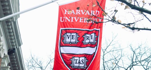
Harvard University and Samsung have settled a patent infringement dispute concerning semiconductor manufacturing techniques. On January 28, Harvard dismissed its lawsuit filed in the Eastern District of Texax in August of 2024, waiving rights to refile.
The parties resolved their differences just days before the final response deadline set for January 31, following an extension granted to Samsung in November 2024.
The suit alleged Samsung’s microprocessor and memory product manufacturing infringed on patents by Professor Roy G Gordon’s lab, specifically US7973189 (‘189 patent) and US7560581 (‘581 patent). These patents cover vapor deposition methods like Chemical Vapor Deposition (CVD) and Atomic Layer Deposition (ALD), crucial for creating thin films in semiconductor devices.
Background and technology
Harvard claimed Samsung used proprietary vapor deposition techniques in products such as the Snapdragon 8 Generation 1 microprocessor and LPDDR5X DRAM memory chips. These processes allegedly replicated Harvard’s methods for depositing thin films containing metals like cobalt and tungsten. These metals are essential for forming interconnects and diffusion barriers, ensuring reliable electrical performance, and preventing material diffusion, which is vital for the longevity and efficiency of electronic devices.
Developed over decades by Professor Gordon’s team, these patented processes have significantly influenced semiconductor manufacturing. The ‘189 patent covers novel processes and materials for thin film deposition, while the ‘581 patent focuses on techniques for forming tungsten-containing films. These patents have set industry standards and ensure technological advancements are properly compensated.
The complaint stated Samsung’s manufacturing process for the Snapdragon 8 Generation 1 involved exposing substrates to a gaseous mixture containing cobalt amidinate vapors, forming a cobalt layer on metal interconnects. Analyses using transmission electron microscopy and energy dispersive x-ray spectroscopy confirmed these metal layers. Samsung’s awareness of the ‘189 patent dates back to at least September 16, 2014, when its own patent cited Harvard’s work, indicating the company knew of the technology it was allegedly using. In the case of LPDDR5X DRAM memory chips, Samsung’s process involved depositing a tungsten film using a specific compound for tungsten gates and bitlines. Similar analyses confirmed the presence of tungsten metal layers. These deposition methods are used in high[1]end smartphones like the Galaxy S22 and Galaxy Z Flip5, underpinning the fabrication of microprocessors and memory chips. The overlap between Harvard’s patented processes and Samsung’s techniques was central to the infringement allegations.
Legal context
Harvard’s legal action aligns with its commitment to defending its innovations. The university has previously litigated against semiconductor manufacturers like Micron and GlobalFoundries over similar allegations related to Professor Gordon’s research, resulting in settlements in 2017 and 2018. The lawsuit was filed in the U.S. District Court for the Eastern District of Texas, known for its plaintiff’s friendly stance in patent disputes. This venue has also seen actions from institutions like the California Institute of Technology and the University of Connecticut, reflecting a trend in academic efforts to secure fair compensation for technological contributions.
Conclusion
While Harvard has chosen not to pursue further litigation, the case underscores the influential role of academic research in technological innovation. The inclusion of patents like the ‘581 and ‘189 in Harvard’s portfolio highlights the university’s dedication to protecting advanced deposition techniques integral to semiconductor manufacturing. Although the terms of the settlement remain undisclosed, the resolution may have broader implications for how universities and technology companies navigate the complex landscape of patent law and technological innovation.
For Samsung, the settlement allows continued production of advanced devices without the distraction of prolonged legal battles. The resolution highlights the challenge of balancing rapid technological progress with the need to compensate for foundational research.
As semiconductor technologies evolve, disputes over intellectual property rights are likely to continue, prompting discussions about rewarding innovation while maintaining competitive markets.
In summary, Harvard’s settlement with Samsung concludes a complex legal dispute and reinforces the critical importance of academic innovation in shaping industrial practices. While the deposition methods’ technology remains key, the broader implications of the case testify to the enduring impact of scholarly research on the global tech landscape.
Author’s comment
While Harvard has chosen not to pursue further litigation, the case underscores the influential role of academic research in technological innovation.

Written by Mayank Laroia
Co-Founder, PatVerse

You may also like…

China’s push to lead AI-driven communication: patents, innovation, and global competition
On a technical level, one of the most significant trends in the global information and communication industry today is...

Director Review reverses PTAB decision based on contradictory expert testimony in Interactive Communications v. Blackhawk Network Inc.
The USPTO Director's recent reversal of a Patent Trial and Appeal Board (PTAB) Final Written Decision in Interactive...

Survival of the fittest: Strava sues Garmin for patent infringement
Fitness app company Strava has recently made waves in the running and cycling communities after suing Garmin for...
Contact us to write for out Newsletter